Most ops folks take the “typical” computer boot process for granted. On today’s typical x86 laptops, desktops, and servers, the process appears pretty straightforward. Push the power button, wait for the BIOS/UEFI to do some magic, and the computer will attempt to start an operating system from whatever media it’s configured to use. If you want to boot from a new media type (such as USB, SATA, and NVMe drives, or PXE network boot), it’s typically as easy as adding the boot media to your computer, changing an easy to configure option in the BIOS, and continuing like normal.
Other CPU architectures, and in general single board computers (SBCs), do not have these luxuries. Generally speaking, when a SBC boots, board designer and/or operator must directly provide the CPU with all code and configuration for the entire boot process, often down to the very first instruction that is executed. This is usually more than a simple “run the operating system on hard drive one”. It typically entails telling the CPU how to load the operating system, as well as configuring the hardware for this process. In this post, I will cover what this process looks like for the RK3588, and I will show how I added NVMe boot support to the Blade 3 board.
Typical non-x86 boot process
Very generally speaking, the boot process for boards based on non-x86 CPUs (such as ARM CPUs, like the RK3588) looks something like this:
- Power physically connected to the board. Certain very low power circuits may turn on, such as recharging real time clock (RTC) batteries.
- A power button/similar is pressed. Some boards (like Raspberry Pis) skip this step.
-
Power regulators turn on. These convert the input power to the voltages needed by the rest of the board. There is also often power control logic that handles “power staging”, where certain “power domains” are turned on according to a timing diagram. A “power domain” is one or more power supplies (such as a regulator) that are centrally controlled to provide power at a specific voltage to certain components, or specific circuits inside components. This allows for enabling/disabling specific circuits affecting others. For example, the power domain for a GPU could be disabled for boards with no video output.
For most CPUs, it is required that specific power domains turn on in a specific order. If they are not turned on in the correct order then the device could fail to start properly or become damaged. Below is a timing diagram that shows the power startup sequence for a RK3588 SBC.
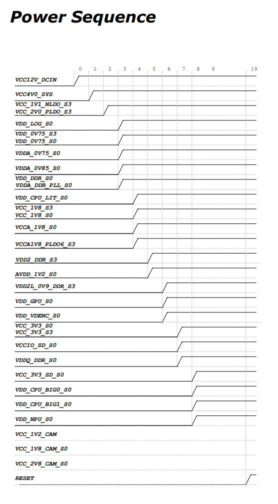
Subset of the RK3588 power domains. - The CPU turns on and moves to a “startup” state. This usually involves setting registers (such as the program counter) to specific values and converging internal hardware state machines to specific states. The details of this process vary from processor to processor. The clock speed of the processor in this state is usually the clock speed of the default clock source attached to the main/master clock PLL. This is often driven by an internal RC oscillator at 32.768 kHz, or an external crystal at 32.768 kHz, 12, 40, 66, or 80 MHz. These frequencies are often picked based on the requirements of other devices in the CPU (such as USB or PCIe), which require specific clock frequencies to drive the hardware.
- The CPU starts executing instructions at whatever address the program counter initializes to. Most CPUs will have either a boot ROM (“burned” into the silicon by the CPU manufacturer), or flash memory. The program counter will generally be set in step (4) to point to a specific address in one of these. The flash memory can usually be programmed by the board manufacturer and/or end users via a JTAG interface. Both boot ROMs and CPU-internal flash storage are typically very small, measured in the kilobyte range. Many documents will refer to the code executed in this step as a “stage 1 bootloader”.
- The stage 1 bootloader may perform very minimal hardware configuration, and then loads another, larger bootloader stage into memory. This hardware configuration may include enabling power domains, assigning certain pins to “peripherals”1, turning on power domains, and enabling and configuring peripherals. It usually involves setting up external RAM. After this next “stage 2” bootloader is loaded into memory, the stage 1 bootloader executes it.
-
The stage 2 bootloader is usually in charge of loading and starting the operating system. It performs a similar function as the stage 1 bootloader, but it can configure more hardware and perform more complex loading operations as the code is not as space constrained. This bootloader stage performs a lot of functions that typical computer’s BIOS would handle, such as configuring DRAM, increasing the CPU clock multipliers, and setting up CPU-external busses. This stage will sometimes have some limited filesystem reading capabilities, often only able to read FAT filesystems. U-Boot is often used for this stage, as it greatly reduces the amount of code that needs to be written/maintained for complex boot operations.
Assuming Linux is the target operating system, the stage 2 bootloader will typically load a “device tree blob” (DTB) into RAM from external storage. This “device tree” is used to tell the Linux kernel about what devices exist, what driver/kernel module should be used for them, and how they should be configured. After the DTB is loaded, a kernel image is loaded as well2. Lastly, the bootloader configures the CPU registers with the address of the DTB and jumps to the loaded kernel. The kernel’s expectation of the CPU registers at boot time is available here.
RK3588 boot process
The RK3588 roughly follows the above boot process, with a few exceptions. The first stage bootloader is implemented via a boot ROM. The next step is a “secondary program loader” (SPL) followed by a “ternary program loader” (TPL) which then loads U-Boot. The SPL and TPL are closed source binary blobs provided by the CPU manufacturer (Rockchip). They are combined in the bootloader build process, so I will refer to them collectively as the “second stage bootloader” for the remainder of this document. This second stage bootloader is typically combined with U-Boot during the firmware build process.
Upon power on, the boot ROM is executed. Assuming the SARADC_IN0_BOOT pin is not pulled down, the boot ROM jumps to sector 64 (0x40h) of an attached SD card, eMMC flash, or SPI flash, depending on the voltage at the SARADC_IN0_BOOT pin. Most boards implement this as a series of switches, when it is configurable by the end user. Board designers should implement this as a voltage divider referenced from the VCCA_1V8_S0 rail according to page 26 of the hardware design guide.
The second stage bootloader expects the next stage to be loaded at sector 61384 (0x4000h). This is where the compiled U-Boot image should be placed.
The boot process looks as follows:
             Power on event
                    |
                    V
              Boot ROM runs
                    |
                    V
    Boot ROM jumps to selected device,
 second stage bootloader (SPL, TPL) runs
                    |
                    V
U-Boot runs, loads kernel and device tree
                    |
                    V
               Kernel runs
Recovery mode
The stage 1 bootloader can switch to a special “MaskROM” mode during initial power up if the SARADC_IN0_BOOT pin is pulled low during startup. When booting in this mode, the RK3588 can be connected to another computer via one of the USB ports (labeled USB0/ADB on the Blade 3). The RK3588 shows up as a 2207:350b Fuzhou Rockchip Electronics Company USB device, and can be accessed via the rkdeveloptool34. This tool can be used to list basic board-specific information such as the CPU ID, serial number, and attached flash storage information. The tool can also be used to write to flash storage and is the primary way of updating the boot process. Having access to this tool is critical for recovering the board after a botched bootloader/firmware update.
Here is the process to access the CPU in MaskROM mode:
- Remove all power to the board.
- Pull the
SARADC_IN0_BOOTpin low (usually via a “MaskROM” button or switch on the board). - Apply power to the board. It should boot almost instantly (<1s). The
SARADC_IN0_BOOTpin can be released now, or at any later point. - Connect the CPU to a host computer via a USB cable connected to the MaskROM USB port (USB0/ADB on the Mixtile Blade 3).
-
Verify that the device is attached in MaskROM mode by running the following:
 vscode ➜ / $ lsusb | grep Rockchip
 Bus 003 Device 028: ID 2207:350b Fuzhou Rockchip Electronics Company
The bus and device address may differ. If no entry is listed, abort and diagnose the problem.
- Download rkdeveloptool and build it, following the instructions in the readme file.
-
A special loader program must be uploaded to the CPU prior to running any other commands via rkdeveloptool. Build it as follows:
 git clone --depth 1 --single-branch --branch master https://github.com/rockchip-linux/rkbin.git
 cd rkbin
 ./tools/boot_merger RKBOOT/RK3588MINIALL.ini
This builds the
rk3588_spl_loader_v1.12.112.binfile. Note that this file name may vary a bit over time, as the manufacturer pushes out new versions. -
Upload the miniloader to the CPU:
vscode ➜ /path/to/rkdeveloptool $ sudo rkdeveloptool db "/path/to/rk3588_spl_loader_v1.12.112.bin" Downloading bootloader succeeded. -
The CPU can now be accessed via rkdeveloptool:
 vscode ➜ /path/to/rkdeveloptool $ sudo rkdeveloptool ppt
 Partition Info(gpt):
 NO  LBA        Size       Name
 01  0x00008000 0x00100000 primary
 02  0x00108000 0x1d0f7fdf
New Blade 3 boot process
The version of U-Boot that ships with the Blade 3 boards does not support NVMe OS kernel boot. If I want the kernel and root filesystem to exist on the NVMe drive, then I need to patch U-Boot to support this, and I need to build a new firmware image. When I’m done, the boot process should look like this:
             Power on event
                    |
                    V
              Boot ROM runs
                    |
                    V
     Boot ROM jumps to onboard eMMC,
 second stage bootloader (SPL, TPL) runs
                    |
                    V
U-Boot (stored on eMMC) runs, loads kernel
    from NVMe and device tree from eMMC
                    |
                    V
               Kernel runs
This keeps the OS entirely on the NVMe drive, and the board-specific code itself entirely on the onboard eMMC flash. Taking this approach allows for changing and upgrading the OS without affecting the low-level board specific boot process.
I want all the boot sections to be accessible by the OS. This will allow for easy installation of firmware updates and configuration changes in the future. To accomplish this, I’ll lay out the disk with a separate GPT partitions for each section. The kernel will treat each each partition as a separate device, allowing me to easily mount the section (in the case of the boot configuration partition), or write to it directly (for the SPL/TPL and U-Boot partitions).
When completed, the eMMC storage layout should look like this:
+----------------------------------------+ Sector 0 (0x0h)
|         Protective MBR (LBA 0)         |
+----------------------------------------+ Sector 1 (0x1h)
|           GPT header (LBA 1)           |
+----------------------------------------+ Sector 2 (0x2h)
|   GPT entries (LBA 2 - 33, inclusive)  |
+----------------------------------------+ Sector 34 (0x22h)
|          Empty space, not used         |
+----------------------------------------+ Sector 64 (0x40h)
|               Partition 1              |
|             SPL/TPL binary             |
|    1 MB space, unused spaced zero'd    |
+----------------------------------------+ Sector 2112 (0x840h)
|         Empty space, not used          |
| CPU manufactuerer specifies additional |
|   partitions here, but are not needed  |
+----------------------------------------+ Sector 16384 (0x4000h)
|               Partition 2              |
|              U-Boot binary             |
|    2 MB space, unused spaced zero'd    |
+----------------------------------------+ Sector 20480 (0x5000h)
|         Empty space, not used          |
| CPU manufactuerer specifies additional |
|   partitions here, but are not needed  |
+----------------------------------------+ Sector 32768 (0x8000h)
|               Partition 3              |
|   Boot configuration files (i.e. dtb)  |
|    64 MB space, unused spaced zero'd   |
+----------------------------------------+ Sector 163840 (0x28000h)
|         Empty space, not used          |
| CPU manufactuerer specifies additional |
|   partitions here, but are not needed  |
+----------------------------------------+ Sector END - 33 (END - 0x21h)
|         Secondary GPT entries          |
+----------------------------------------+ Sector END - 1 (END - 0x1h)
|         Secondary GPT header           |
+----------------------------------------+ Sector END
Building new firmware
As previously mentioned, the version of U-Boot that the Blade 3 boards ship with does not include NVMe support. This version of U-Boot is based off of the CPU manufacturer’s RK3588 SDK, which unfortunately uses an ancient fork of U-Boot with lots of custom code layered on top. Thankfully, another company (Collabora) has put a lot of effort into upstreaming RK3588 support into both U-Boot and the Linux kernel. This includes PCIe 3.0 support. Adding NVMe support to the board should be as “simple” as porting Mixtile’s code/configuration to mainline U-Boot and building the project.
Porting a board to U-Boot is a fairly straightforward process. While the Mixtile’s 2017 fork of U-Boot already has support for the Blade 3, the code base differs enough that I decided to start from scratch. Additionally, some of the files that I’ve been sent by them during a few debugging/support calls do not match the source checked into the public tree, indicating that the vendor has another private fork with additional changes. As outlined here, the following process of adding U-Boot support for any given board looks something like this:
- Create board-specific files
board/<vendor>/<board-name>/- Add board setup code
- Add Makefile that tells U-Boot to compile the board setup code
- Add Kconfig that tells Kconfig what macros to set when U-Boot is configured to build the board. Like the Linux kernel, U-Boot uses Kconfig to define specific macros depending on what options are configured. This file tells Kconfig the values of board-specific macros (such as board and vendor name) that should be set during the build.
include/configs/- Add board header file. Take a look at other boards using the same CPU for examples of what needs to be included here.
arch/<CPU ISA, i.e. "arm">/mach-<;CPU manufacturer>/<CPU model>/arch/<CPU ISA, i.e. "arm">/dts/configs/- Add a defconfig file for the board. This file becomes a Makefile target and is used to setup Kconfig with all the options needed to build a board.
- Build the project, addressing any compilation issues.
- Upload the build, test, and iterate.
Defining the device tree
The most difficult part of this process is getting the device tree files and defconfig correct. As mentioned earlier, the device tree is used to tell the kernel about what devices exist, and what drivers can be triggered to use the devices. This is defined in the dts file linked above. There is also a second device tree that is built and used for U-Boot. This is the built by (automatically) combining the Linux device tree source file, and the U-Boot device tree include file, as outlined here. This device tree is operated on very early on in the boot process, and sometimes requires some special tweaks (that are not required for the kernel) to get U-Boot to run properly.
Creating the device tree files is non-trivial as it requires detailed knowledge of both the board itself, the components on it, and how various hardware busses and protocols work. Fortunately, there is a device tree “include” file that takes care of describing most of the CPU’s resources. By including it, I only need to define the board-specific options. This is a somewhat tedious process so I’m not going to step through the entire process for every device, but I’ll cover how I got NVMe boot working.
NVMe is a software interface that (primarily) communicates over a PCIe bus. The device tree doesn’t (generally) need to be informed about software layers - other layers in the driver stack determine this. The PCIe hardware in the RK3588 is split into two categories: controllers and PHYs. Both of these are typically grouped together by operators as “hardware layer”, but they have separate, distinct functions. The controller implements the data link layer, and the controller side of the transaction and physical layer. The PHY implements line coding/decoding and transceiving the line code symbols over the physical medium. Both must be configured properly to establish a link between between the CPU and another device.
According to the RK3588 technical reference manual (TRM), there are five PCIe 3.0 controllers, two PCIe 3.0 PHYs5, and three PCIe 2.0/SATA/USB 3.0 “ComboPHYs”. The memory map in section 1.1 of the TRM shows that there is a memory-mapped four lane PCIe 3.0 controller at address 0xFE150000, and a two lane PCIe 3.0 controller at 0xFE160000. The Blade 3 schematic shows that these are connected to the SFF-8639 port (J2) on sheet 18. This port connects to the Cluster Box backplane, which includes the M.2 drive slot.
Searching the U-Boot source for 0xFE150000 and 0xFE160000 shows that these controllers are already defined in the RK2588 DTS include file, labeled by pcie3x4 and pcie3x2. The compatibility string is listed as "rockchip,rk3588-pcie", "rockchip,rk3568-pcie", which tells U-Boot and the kernel what drivers to use for these entries. There is no documentation about what properties this supports in the U-Boot tree, but the kernel tree has very thorough documentation on what is required. Based on this, the following properties need to be added to the device tree entry for each controller:
vpcie3v3-supply- this tells the driver what power regulator supplies power to the port, so that the driver can ensure that the target device is powered before initializing it.status- this tells the device tree parser at runtime that the entry is actually enabled. This is common to most device tree entries and is currently set to"disabled".reset-gpios- this shows what pin(s) are used to reset the endpoint PCIe device upon controller initialization.num-lanes- thepcie3x4controller supports up to four PCIe lanes, however only two lanes are attached. This property is used to tell the driver how many should be used.pinctrl-namesandpinctrl-0. I don’t know if these are strictly required, however all the other RK3588 boards list this property for the reset GPIOs. These are another way of specifying what pin(s) are used for GPIO resets.
Most of this information can be pulled from the schematic. The directly relevant portions are shown below:
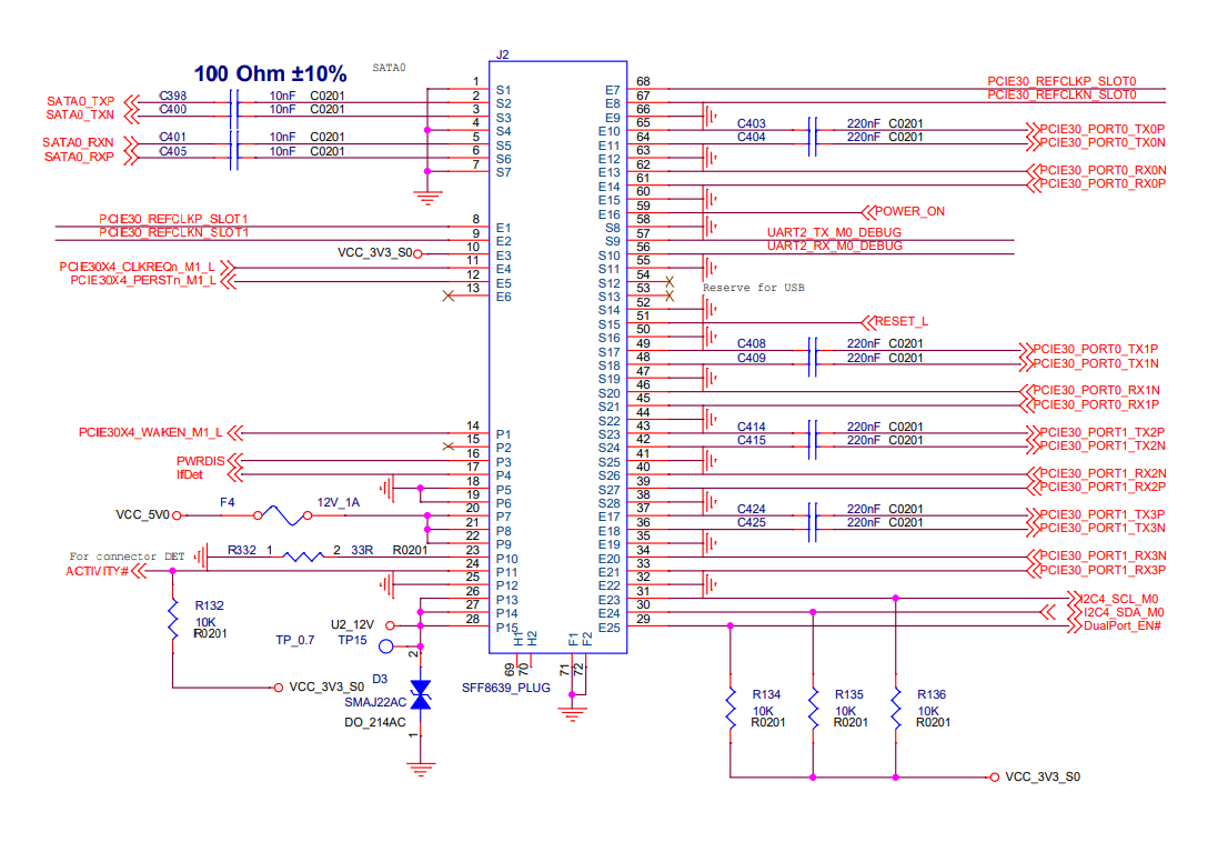
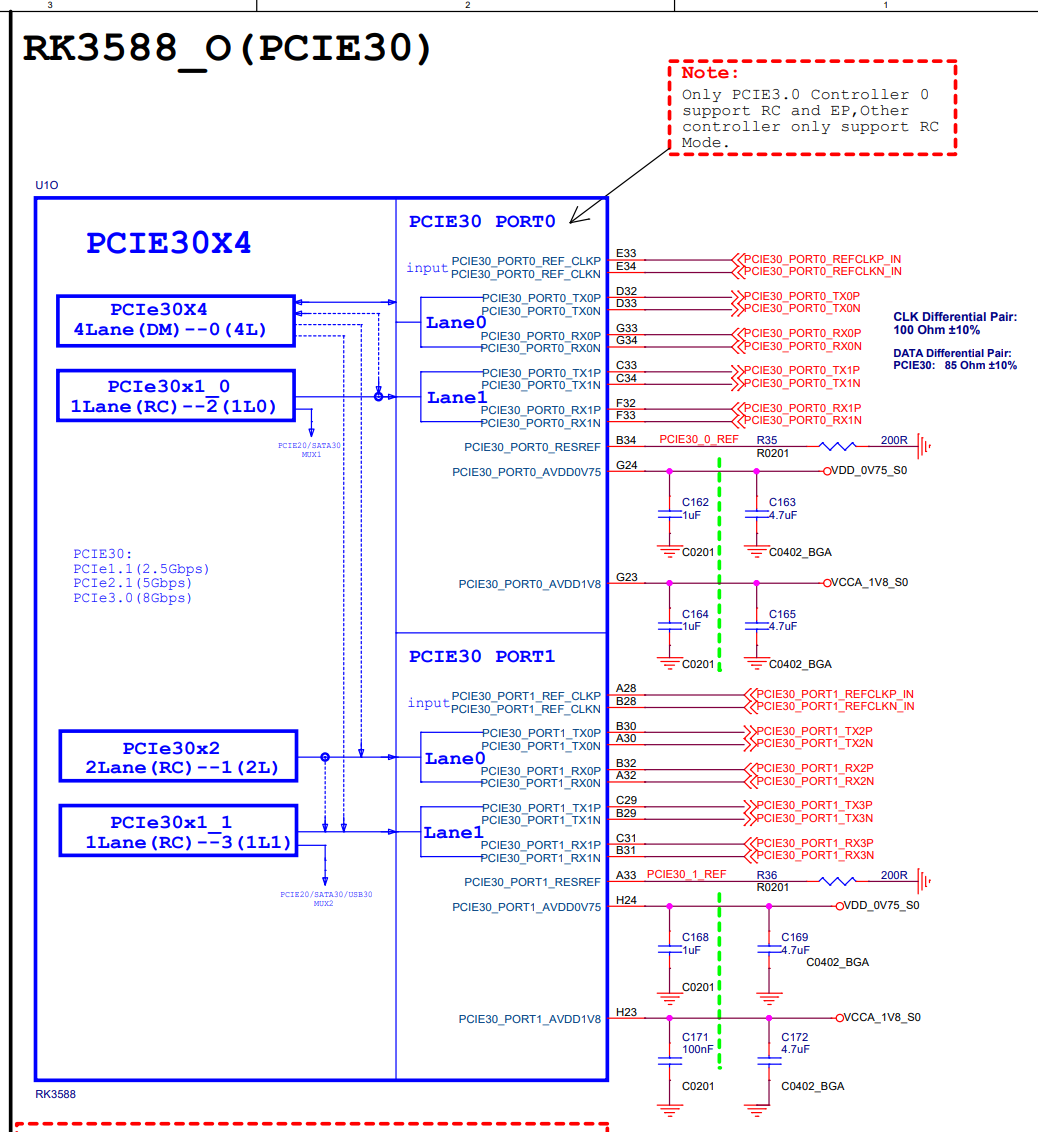
The reset signal is connected to GPIO bank 4, pin B6. This pin is referenced against the VCC_3V3_S0 power rail. PCIe signals are connected to both PHY ports and can be split between four of the five PCIe controllers. From experimentation I found that the Cluster Box uses two sets of PCIe 3.0 x2 links - one for the M.2 drive, and one for the TCP/IP over PCIe backplane.
The device tree entry ends up looking like this:
// The `&` references a label already defined elsewhere in the device tree. The properties listed here will be merged
// by the device tree compiler with the properties already defined in rk3588.dtsi.
&pcie3x4 {                                                  // This is connected to the TCP/IP over PCIe backplane.
	pinctrl-names = "default";                          // This is the only group needed/available for this board.
	pinctrl-0 = <&pcie3_reset>;                         // Reference to the pin configuration.
	reset-gpios = <&gpio4 RK_PB6 GPIO_ACTIVE_HIGH>;     // The reset GPIO is attached to GPIO bank 4, pin B6.
                                                            // The other boards mark this as active high for the same
                                                            // function, which is odd because PERSTn should be active
                                                            // low. Either way, this config works.
	vpcie3v3-supply = <&vcc3v3_pcie30>;                 // This refers to a regulator that I defined elsewhere.
	num-lanes = <2>;                                    // Cut the 4 lane controller down to only two lanes.
	status = "okay";                                    // Enable the device.
};

&pcie3x2 {                                                  // This is connected to the M.2 slot.
	pinctrl-names = "default";
	pinctrl-0 = <&pcie3_reset>;
	reset-gpios = <&gpio4 RK_PB6 GPIO_ACTIVE_HIGH>;     // The connector shares a reset line for both controllers.
                                                            // This is odd, but works.
	vpcie3v3-supply = <&vcc3v3_pcie30>;
	status = "okay";
};

// These tell the driver for another CPU subsystem what the pins should be used for. In most processors, many of the
// pins can be used for multiple functions (such as GPIO, SPI, and I2C, but not all at once).
&pinctrl {
	pcie {
		pcie3_reset: pcie3-reset {
                        // Pretty much the same settings as in reset-gpios. The reset signal is pulled up elsewhere on the schematic,
                        // so the pin does not need the internal pull up resistor enabled.
			rockchip,pins = <4 RK_PB6 RK_FUNC_GPIO &pcfg_pull_none>;
		};
	};
};
The same process is repeated for the PHY. The documentation in the Linux kernel tree states:
data-lanes:
  description: which lanes (by position) should be mapped to which
    controller (value). 0 means lane disabled, higher value means used.
    (controller-number +1 )
  $ref: /schemas/types.yaml#/definitions/uint32-array
  minItems: 2
  maxItems: 16
  items:
    minimum: 0
    maximum: 16
I want to split the lanes by controller, so that lanes 0 and 1 go to the PCIe 3.0 x4 controller (I assume controller 0 or 1), and so that lanes 2 and 3 go to the PCIe 3.0 x2 controller (I assume controller 1 or 2). Therefore, depending on how the controllers are numbered, the entry should look like either:
&pcie30phy {
	data-lanes = <1 1 2 2>;
	status = "okay";
};
or:
&pcie30phy {
	data-lanes = <2 2 3 3>;
	status = "okay";
};
After some extensive testing, neither of these work. When the board attempts to establish a link with the target, it fails for both items. I dug into the U-Boot driver code for the PHY, which looks like this:
#define BIT(nr)			                (1UL << (nr))
#define RK3588_BIFURCATION_LANE_0_1		BIT(0)
#define RK3588_BIFURCATION_LANE_2_3		BIT(1)
#define RK3588_LANE_AGGREGATION			BIT(2)

...

// This reads the device tree property
ret = dev_read_size(dev, "data-lanes");
if (ret > 0) {
    priv->num_lanes = ret / sizeof(u32);
    if (priv->num_lanes < 2 ||
        priv->num_lanes > ARRAY_SIZE(priv->lanes)) {
        dev_err(dev, "unsupported data-lanes property size\n");
        return -EINVAL;
    }

    ret = dev_read_u32_array(dev, "data-lanes", priv->lanes,
                    priv->num_lanes);
    if (ret) {
        dev_err(dev, "failed to read data-lanes property\n");
        return ret;
    }
}

...

// This configures the hardware based on the device tree property
/* Set bifurcation if needed */
for (int i = 0; i < priv->num_lanes; i++) {
    if (!priv->lanes[i])
        mode |= (BIT(i) << 3);

    if (priv->lanes[i] > 1)
        mode |= (BIT(i) >> 1);
}

if (!mode) {
    reg = RK3588_LANE_AGGREGATION;
} else {
    if (mode & (BIT(0) | BIT(1)))
        reg |= RK3588_BIFURCATION_LANE_0_1;

    if (mode & (BIT(2) | BIT(3)))
        reg |= RK3588_BIFURCATION_LANE_2_3;
}

regmap_write(priv->phy_grf, RK3588_PCIE3PHY_GRF_CMN_CON0,
            (0x7 << 16) | reg);
The first half is conceptually simple (it just reads the data-lanes property and does some validation), but the second half is really unclear. One big thing really stands out here: the actual values in the data-lanes array are unused, except for the 0 value (which should indicate a lane is unused). Running through this code, a value of <1 1 2 2> or <2 2 3 3> will always result in all four lanes being bifurcated, all four of the possible PCIe controllers are connected to a separate PCIe lane.
I dug into the TRM and looked up the register associated with RK3588_PCIE3PHY_GRF_CMN_CON0. Table 6.19.2 on page 864 shows that the first three bits of the register are used to configure which lanes are attached to which controller(s). Based on this, the actual value of reg needs to be 0 to split the lanes evenly between the pcie3x4 and pcie3x2 controllers. The only way reg can be 0 when written to the register is if mode is non-zero, but the first four bytes are zero. The only way this can occur is with a value of <n 0 0 0>, where n > 0. This will result in mode being set to a value of 0b01110000, due to an off by one error in the mode setting logic.
I’m fairly certain that I’m the first person to test this specific case, and I’m also pretty certain that this is a bug in the upstream code. I will probably file a patch sometime in the next couple of months to fix it.
The final value for the PCIe 3.0 DTS entries looks like this:
&pcie3x4 {
	pinctrl-names = "default";
	pinctrl-0 = <&pcie3_reset>;
	reset-gpios = <&gpio4 RK_PB6 GPIO_ACTIVE_HIGH>;
	vpcie3v3-supply = <&vcc3v3_pcie30>;
	num-lanes = <2>;
	status = "okay";
};

&pcie3x2 {
	pinctrl-names = "default";
	pinctrl-0 = <&pcie3_reset>;
	reset-gpios = <&gpio4 RK_PB6 GPIO_ACTIVE_HIGH>;
	vpcie3v3-supply = <&vcc3v3_pcie30>;
	status = "okay";
};

&pinctrl {
	pcie {
		pcie3_reset: pcie3-reset {
			rockchip,pins = <4 RK_PB6 RK_FUNC_GPIO &pcfg_pull_none>;
		};
	};
};

&pcie30phy {
	data-lanes = <1 0 0 0>;
	status = "okay";
};
This isn’t much code, but it took a lot of effort to get working. The remaining device tree entries that I added took significantly less effort.
Building the defconfig
Like the Linux kernel, U-Boot is complex enough that a handful of Makefile args or autotools flags cannot feasibly capture all the options required to build the project. This is where Kconfig comes in. Kconfig provides a nice, easy to use set of tools to manage configuration options and use them at build time. It also makes heavy use of dependencies between options. For example, before enabling NVMe support, PCIe support must be enabled. Later, these config options are mapped to C macros that the preprocessor includes when building the project.
The defconfig file is used to populate the .config file that Kconfig uses to define macros for the actual build. Getting the right values is largely trial and error, using other similar boards as a starting point. To write the defconfig for the Blade 3 board I ran make menuconfig (which launches a nice TUI for configuration) and went through every single option to determine if it should be enabled for this board. This probably isn’t the most efficient way to go about it, but the process works.
Creating the disk image
With U-Boot properly configured, the only remaining thing is to build the project and upload a disk image. If you only care about getting a build going, see the Earthly Earthfile I wrote here. Building the image can be broken down into a tree of dependencies:
- Build eMMC image
- Create partition table and partitions
- Write the second stage bootloader (SPL/TPL) to the first partition
- Build the second stage bootloader
- Write the third stage bootloader (U-Boot) to the second partition
- Build U-Boot
- Write boot config files (such as the device tree blob) to the third partition
- Create FAT32-formatted image file
- Write copy the boot config files to it
U-Boot is pretty easy to build. Building U-Boot also conveniently builds the second stage bootloader and compiles the device tree. After configuring U-Boot and installing its (numerous) build dependencies, it can be built with:
# Download the SPL and TPL files from the CPU manufacturer's GitHub repo
wget https://github.com/rockchip-linux/rkbin/raw/master/bin/rk35/rk3588_ddr_lp4_2112MHz_lp5_2736MHz_v1.12.bin && \
wget https://github.com/rockchip-linux/rkbin/raw/master/bin/rk35/rk3588_bl31_v1.40.elf

# Do the actual build
make -j"$(nproc)" CROSS_COMPILE=aarch64-linux-gnu- \
    ROCKCHIP_TPL=./rk3588_ddr_lp4_2112MHz_lp5_2736MHz_v1.12.bin BL31=./rk3588_bl31_v1.40.elf
A minute or two later U-Boot spits out several files to the root of the source tree. There are three files that are needed:
idbloader.img- This is the built second stage bootloader, ready to be written to the first partition.u-boot.itb- This is the built U-Boot binary, ready to be written to the second partition.u-boot.dtb- This is the compiled device tree blob, ready to be copied to the third FAT32 partition.
Thanks to dosfstools and mtools, it is easy to create a FAT32 image file and manipulate it:
# Create 4MB 0'd out file
PARTITION_SIZE_BYTES=$(( 8192 * 512 ))
IMAGE_FILE_PATH="./boot-config.img"
truncate --size=$PARTITION_SIZE_BYTES "$IMAGE_FILE_PATH"

# Format the image file as a FAT32 file system, and label it as "boot-config"
mkfs.vfat -F32 -n "boot-config" --mbr=no "$IMAGE_FILE_PATH"

# Copy the device tree blob to the image file
mcopy -i "$IMAGE_FILE_PATH" ./u-boot.dtb ::
Image file contents:
$ mdir -i "$IMAGE_FILE_PATH"
u-boot   dtb     87632 2024-01-23   9:33
        1 file               87 632 bytes
                         65 970 688 bytes free
This could also be accomplished by mounting the image file via a loopback device, but this would require root privileges. This approach can be accomplished with only typical user permissions.
The image file itself can be created in a similar manner:
SECTOR_SIZE=512
# Calculated from https://opensource.rock-chips.com/wiki_Partitions
SECT_COUNT=$(( 1 + 63 + 7104 + 512 + 384 + 128 + 64 + 8192 + 8192 + 8192 + 229376 + 33 ))
IMAGE_SIZE_BYTES=$(( SECTOR_SIZE * MIN_SECT_COUNT ))

# Record where the partitions start so that they can be written to directly later
IDBLOADER_FIRST_SECTOR=64
U_BOOT_FIRST_SECTOR=16384
BOOT_CONFIG_FIRST_SECTOR=32768
BOOT_CONFIG_END_SECTOR=163839
BOOT_CONFIG_PARTITION_SIZE_BYTES=$(( (BOOT_CONFIG_END_SECTOR - BOOT_CONFIG_FIRST_SECTOR + 1) * SECTOR_SIZE ))

# Create the image file and setup a partition table
IMAGE_FILE_PATH="./firmware.img"
truncate --size=$IMAGE_SIZE_BYTES $IMAGE_FILE_PATH
parted --script "$IMAGE_FILE_PATH" \
    # Create the GUID partition table
    mklabel gpt \
    # Set the unit for the remainder of the command to "sectors"
    unit s \
    # Create the SPL/TPL partition that idbloader.img will be written to
    mkpart primary $IDBLOADER_FIRST_SECTOR 2111 \
    # Create the U-Boot partition that u-boot.itb will be written to
    mkpart primary $U_BOOT_FIRST_SECTOR 20479 \
    # Create the boot configuration partition that the device tree and boot script will be written to
    mkpart primary fat32 $BOOT_CONFIG_FIRST_SECTOR $BOOT_CONFIG_END_SECTOR \
    # Name the partitions
    name 1 "idbloader" \
    name 2 "u-boot" \
    name 3 "boot-config" \
    # Set the boot config partition GUID to "boot"
    set 3 boot on

# Label the boot-config partition as a /boot partition
sfdisk --part-type "$IMAGE_FILE_PATH" 3 "Linux extended boot"
The partitioned image file is structured as follows:
$ sfdisk --dump "$IMAGE_FILE_PATH"
label: gpt
label-id: 0C76A2B1-F72E-418B-8453-74BE644F9D44
device: firmware.img
unit: sectors
first-lba: 34
last-lba: 262207
sector-size: 512

firmware.img1 : start=          64, size=        2048, type=0FC63DAF-8483-4772-8E79-3D69D8477DE4, uuid=34AA2AEE-596D-4762-8E3B-3214D588681E, name="idbloader"
firmware.img2 : start=       16384, size=        4096, type=0FC63DAF-8483-4772-8E79-3D69D8477DE4, uuid=11B91032-1519-40F0-B26E-3FA42F565372, name="u-boot"
firmware.img3 : start=       32768, size=      131072, type=BC13C2FF-59E6-4262-A352-B275FD6F7172, uuid=53E4093E-EA04-4096-96AD-85CFFD4F153F, name="boot-config"
These partitions line up with the start and end sectors listed above.
The dd command can now be used to write the contents of each partition to the appropriate places:
# Write the partition image file
dd of=$IMAGE_FILE_PATH bs=$SECTOR_SIZE conv=notrunc if=./idbloader.img seek=$IDBLOADER_FIRST_SECTOR
dd of=$IMAGE_FILE_PATH bs=$SECTOR_SIZE conv=notrunc if=./u-boot.itb seek=$U_BOOT_FIRST_SECTOR
dd of=$IMAGE_FILE_PATH bs=$SECTOR_SIZE conv=notrunc if=./boot-config.img seek=$BOOT_CONFIG_FIRST_SECTOR

# Force any async writes to complete
sync --file-system $IMAGE_FILE_PATH
The image file is now 100% complete and ready for upload.
Flashing the new firmware
The flashing process is really easy now that the firmware and flashing tool are both built. After entering MaskROM mode, the following will upload the file:
./rkdeveloptool db rk3588_spl_loader.bin    # Upload the miniloader
sleep 5                                     # Sleep while the bus re-enumerates
./rkdeveloptool wl 0x0 firmware.img         # Upload the image to the eMMC, and write it to sector 0
While still in MaskROM mode, the partition table can be printed:
$ ./rkdeveloptool ppt
**********Partition Info(GPT)**********
NO  LBA       Name
00  00000040  idbloader
01  00004000  u-boot
00008000  boot-config
Note that the LBA are sectors in hex notation. This matches up with the desired partition layout.
If desired, everything in this post can be built and flashed by checking out this branch and running sudo earthly +flash-device with the targeted Blade 3 attached in MaskROM mode.
End results
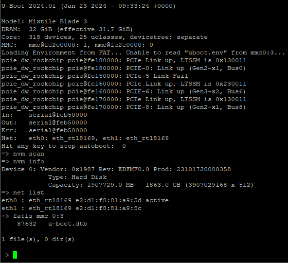
The board boot to U-Boot successfully and appears to support everything I was looking for. For some reason the PCIe switch does on the backplane does not enumerate (this is the “Link Fail” in the picture), but this isn’t a problem for boot. If it doesn’t work in the OS then I will debug further.
Everything else shows up properly. The RT8169 driver works for the RT8125 NICs, the 2TB M.2 NVMe drive is recognized (although it is currently unformatted), and the dual Coral TPU card that I inserted into the MiniPCIe slot is able to establish a link. The boot-config partition is also readable.
After I install an OS on the M.2 drive (in a future post), U-Boot should use the bootflow command to discover the OS and boot it.
Wrapping up
This portion of the project took longer than I thought (about 3 weeks in total including writing this post), but I’m satisfied with the end results. I was able to add firmware-level support for the Blade 3 board to U-Boot without assistance from the manufacturer. I’m pretty sure that I’m also the first person to get RK3588 PCIe 3.0 bifurcation working in this configuration on modern U-Boot (or modern Linux, as the driver logic is identical), or else I probably wouldn’t have hit the PHY bug discussed earlier.
In unrelated news, I got a replacement for a failing Cluster Box board that has been preventing me from doing a higher-level performance/general experience writeup of the whole setup. I’ll probably write a post about that next.
-
In the embedded engineering world, “peripheral” usually refers to a hardware function or bus inside a chip. For example, a USB controller, SPI master, and SD card controller would all be considered peripherals. ↩
-
If the kernel is stored in flash that supports execute in place, then it doesn’t necessarily have to be copied to RAM. ↩
-
This is a Radax fork of the upstream Rockchip tool with a couple of minor fixes. ↩
-
There is a closed source Windows alternative available here. This driver is also needed on Windows. ↩
-
I later found out that both the U-Boot and Linux kernel drivers treat these as one single PHY. ↩